
Why TPU Can Cut Costs by 80% at Scale & Google's Balance Sheet Strategy Hints Aggressive Market Move


For years, the math was simple: NVIDIA’s CUDA ecosystem was a mandatory cost of entry, securing them estimated 80%+$ gross margins on GPUs and forcing tech giants to pay a massive silicon premium. Today, that economic model is under its most serious challenge yet. The fight has shifted decisively from raw speed to Total Cost of Ownership (TCO), driven by the sobering reality that AI inference costs will soon outweigh training costs by 15x or more over a model’s lifecycle.
To counter this, Google developed the TPU an ASIC built to be ruthlessly efficient. Now, they are weaponizing this externally. The market is currently witnessing Google’s three unprecedented strategic moves that signal a fundamental shift in compute economics:
Google’s Balance Sheet Backstop strategy
Anthropic Deal
Meta Hedge
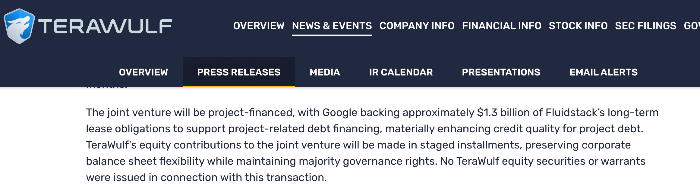
First, Google is deploying its Balance Sheet Backstop strategy: using its vast financial capacity to guarantee billions of dollars (e.g., a reported $1.3 billion backstop for partners like TeraWulf and Fluidstack) to build new, non-Google data centers.
This move is not charity; it is a calculated financial maneuver designed to solve Google’s two biggest problems in the AI race:
Speed-to-Market: Google needs vast amounts of new TPU capacity deployed faster than it can build its own data centers. Partnering with a company like TeraWulf, which already owns power contracts and infrastructure, allows for rapid expansion (e.g., the first phase was expected to come online within months).
External Distribution: By placing TPUs outside of GCP through “neoclouds” like Fluidstack, Google lowers the entry barrier for smaller AI companies and developers who might be wary of full GCP vendor lock-in, thus accelerating TPU ecosystem adoption and directly challenging NVIDIA’s installed base.
Google is using its balance sheet to subsidize the CapEx required to stand up an alternative to the NVIDIA/AWS/Azure cloud ecosystem, a move that provides a low-cost, high-efficiency compute option that structurally undercuts the high-margin NVIDIA model.
Second, the foundational model builder Anthropic has made a clear, strategic commitment to buy up to $1 M Google TPUs. This deal, valued at billions, provides critical third-party validation that the TPU offers superior price-performance, delivering up to 4x better cost-performance than NVIDIA GPUs for certain Large Language Model (LLM) tasks.
Third, the threat is magnified by The Meta Hedge: one of NVIDIA’s largest existing customers, Meta, is reportedly in advanced talks to integrate TPUs into its own data centers starting in 2027. This signifies that the cost pressure from TPUs is too significant to ignore, forcing even the most committed GPU users to seek a major hedge and potentially divert billions in future spending away from NVIDIA. The core investment question is no longer about raw power, but about which architecture—the general-purpose flexibility of the GPU, or the specialized, TCO-optimized ASIC backed by Google’s aggressive financial strategy—will secure the lowest perpetual operating cost for the next decade of AI deployment.
We also see venture and investor excitement shifting: Berkshire Hathaway took a stake in Alphabet in 2023/2024, which many interpreted as a bet on Google’s AI strategy Buffett, known for favoring economic “moats,” likely saw Google’s vertical integration as a moat that can challenge Nvidia’s.
We have seen no shortage of blogs and news articles comparing the technical architectures and benchmark performance of TPUs versus GPUs. That is not the purpose of this article. Instead, we are approaching the question from a C-suite perspective, focusing on economic outcomes, capital allocation, and long-term operating leverage—how these platforms change total cost of ownership, risk, and strategic flexibility at scale, rather than which wins a micro-benchmark.
In today’s article, we’ll dig into the questions that have dominated recent client conversations:
Simulate a C-Suite Total Cost of Ownership (TCO) discussion between the VPs of Infrastructure/AI at Anthropic (a committed TPU user) and Meta (a large, hedging GPU user). Which accelerator—NVIDIA’s or Google’s —delivers the superior TCO in three distinct scaling scenarios: Base Cluster (1K Accelerators), Medium Cluster (10K Accelerators), and Hyperscale Cluster (100K+ Accelerators)?
What is the specific bill of materials (BoM) and supply chain architecture of a modern Google TPU Pod (e.g., Ironwood v7)? How does Google’s vertical integration—from silicon co-development to the interconnect fabric—create an economic moat that provides both significant unit cost advantage and unmatchable supply chain predictability?
Software Ecosystem: CUDA vs. XLA – Will Customers Face Lock-In? Can you run Hugging Face (PyTorch) models on TPU? What is the downsides for companies to use TPU vs. Nvidia across the dimensions ?
Please note: The insights presented in this article are derived from confidential consultations our team has conducted with clients across private equity, hedge funds, startups, and investment banks, facilitated through specialized expert networks. Due to our agreements with these networks, we cannot reveal specific names from these discussions. Therefore, we offer a summarized version of these insights, ensuring valuable content while upholding our confidentiality commitments.
What a “TPU Pod” Actually Is (Rack-Level, Not Chip-Level)
When Google sells TPUs, it is not selling “a chip.”
A TPU Pod is a vertically integrated system in which compute, memory, networking, cooling, and software are designed together and operated as a single economic unit. Thousands of accelerators behave like one machine.

Source: Part of an Ironwood superpod, directly connecting 9,216 Ironwood TPUs in a single domain.
The key to understanding Google’s TPU strategy is that all layers matter, simultaneously. A TPU Pod is not a chip decision; it is a full‑stack system that spans accelerator trays (compute and memory), intra‑rack fabric and host nodes, inter‑rack optical networking, power delivery and direct liquid cooling, and a pod‑level runtime and scheduler that treats thousands of accelerators as one logical machine.
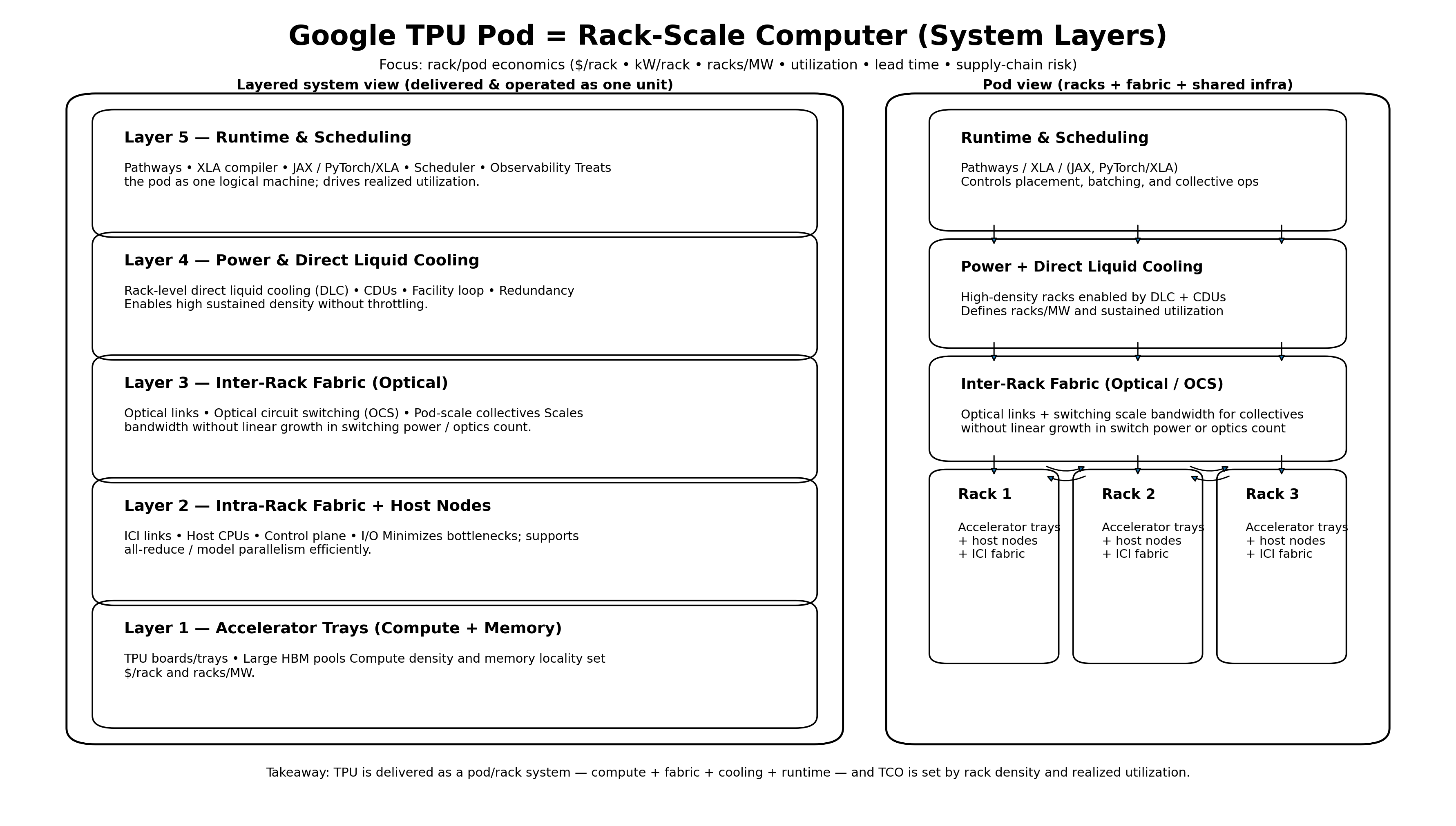
These layers are co‑designed and deployed together, and the economic outcome—$/rack, racks per megawatt, utilization, and speed of deployment—is determined by how well they work as a unified system. Focusing on any single layer in isolation misses the point: Google’s advantage emerges from integrating all layers into a rack‑scale computer with predictable cost and performance at scale.
Let’s look at the layers in detail before we get into TCO scenarios.
